About Antenna Matching
Over the years many of my clients (about 1/2) have needed assistance with antenna matching. For short range-RF products (Zigbee, Bluetooth and WiFi) a poorly matched antenna shows up as a weak radio link. For cellular products a poorly matched antenna usually shows up as a Total Radiated Power (TRP) failure. If your product fails TRP it will not be accepted onto a carrier’s network and you have no way for your customer to use your product.
Antenna matching involves creating a passive network between the RF electronics and the antenna. A perfect match results in the power amplifier seeing the complex conjugate of its impedance across the frequency range(s) of interest and ditto for the antenna.
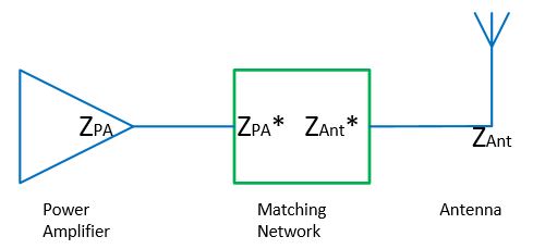
The Matching Network Creates Two Complex Conjugate Matches
While many semiconductors and antennas have published performance specifications (S11, VSWR) when they are placed into your product things will not work as specified. This is usually due to the antenna’s physical environment. Both metal and plastic in the vicinity of an antenna will change its resonance points and behavior. For large environment changes an antenna redesign (lengthen or shorten for example) is needed to move the resonance point back to band center. Once that is done you still typically need to match the impedance. This antenna matching effort is usually required when using standard antenna designs such as a PCB style inverted F antenna or any of the common ceramic, FR4 or flexible PCB antennas available from Antenova, Ethertronics, Taoglas and the like as you have only modest control over the antennas tuning.
If you have access to a Vector Network Analyzer then you can learn to solve your own antenna matching problems. To help you learn to do this I have created an Antenna Matching course that will teach you what you need to know and do to match your antenna to your RF electronics. Of course if you do not have access to the required test gear, or just do not have the time or inclination I will be happy to do perform this service for you.
There are three easy things that you can use to reduce the time required to match an embedded antenna when you lay out your PCB.
- Place space for small RF components near your antenna. For a narrow single band a basic Tee or PI structure will suffice as most matching networks will be a Low-Pass filter. (Also useful for suppressing harmonics).
- Leave space for a small RF connector (like a U.FL connector) that can be left out during production
- Figure out in advance how you would route a small coaxial connector to the RF output trace and leave visible ground plane nearby. This is useful for reducing the effects of the RF test cable on the antenna behavior.
Good luck with your product and be sure to check out our short video here.